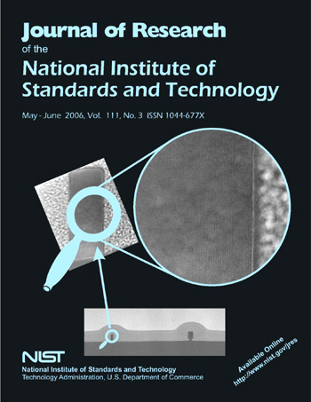
Cover Explanation:
The cover illustration, from the paper by Cresswell et al. on page 187, shows an HRTEM image of a
narrow silicon feature. The width of this feature was determined to be 45.67 nm with an expanded uncertainty of
0.59 nm, by counting the lattice-planes of the silicon. The feature was fabricated such that the top surface
is a (110) plane and the sidewalls are separated by parallel (111) planes. The (111) plane spacing is exactly
0.313 560 137 nm with a standard uncertainty of +/– 0.000 000 009 nm. The (111) planes are imaged as lines,
rather than as individual atoms, to facilitate counting the lattice. This is accomplished by rotating the sample
slightly along the axis of the (111) planes. If this rotation is along exactly the correct axis, the images of the atoms
are “smeared” into lines. Cover arranged by C. Carey.